

It is widely believed in the industry that if a parameter during solder paste printing can be precisely not potentially 60% of the process deference can be avoided. Hence every stage from equipment selection, installation setting the process parameters, using the right tool and following the set process parameters needs to be precise.
The function of solder paste printing equipment is to deposit the right volume of solder paste on PCB pads on which components need to be solder Precise volume of solder paste is important because: 1) Solder Paste has “tackiness” property which helps hold the surface mount component in its place. 2) Proper solder builds up on component termination which ensures adequate electrical connection as well as physical support during the life of the product.
Key tool used during this process are 1) Squeeze 2) Stencil Squeeze can be made of stainless steel or from a combination of stainless steel and rubber. Squeeze manufactured from stainless steel is comparatively expensive but has a much higher serviceable life.
Stencil, as the name suggests is a stainless steel plate typically 4mils up to 7 mils in thickness with aperture openings wherever solder paste deposition is required on the PCB. The stencil is manufactured for a specific design of the PCB hence the PCB CPN along with the revision is etched on the surface of the stencil. Depending on the production requirement multiple versions of the same design of stencil is fabricated so that it can be used in concurrence.
Hence, it is very important to track the number

Considering the thinness of the stencils, it needs to be handled a proper racking system. The stencils, which needs to be used in the shop-floor for manufacturing operations are kept in a rack while___ is placed within the shop-floor itself. For rest of the stencils designated area outside the shop-floor, typically in an area within warehouse is used. The product data management team of the electronics manufacturer keeps a track at stencils available, the obsolete stencil designs are purged from the storage and sent for re-cycling. Further if the electronic manufacturer is manufacturing for both leaded and lead-free processes, the corresponding proceed stencil needs to be identified separately and stacked separately. Typically stencils which are used in lead-free process have green coloured frame which helps easily identify the process in which it will be used.
The stencil apertures are cut using laser cutting machines ensuring precise cut of the aperture. As mentioned earlier, precise volume of solder paste deposition on the solderable lands of the PCB in very important. The stencil thickness is determined by the volume of solder paste that will be deposited on the PCR lands. For some component packages additional volume of solder needs to be deposited, in such cases the specific aperture area has increased thickness and such apertures are referred as “step-up” stencil aperture. On the other hand, some components need lesser Volume of solder paste deposition in that case the stencil aperture of those components have reduced thickness and are referred to as “step-down” stencil aperture. PCB land to aperture of stencil is an important ratio, this ratio is well defined based on the manufacturing process leaded or lead-free stencil design guideline IPC-XXX
Since solder paste is used to deposit using a stencil the solder balls of the solder paste tends to stick to the component aperture openings hence typically after every 3 to 7 “printing” the stencil needs to be with cleaned with lint free paper or lint free cloth. Post completion of printing operation at the end of the shift the stencil solvent and then dried using compressed air. Such cleaning can be done manually or using specialized equipment called stencil cleaning equipment.
Sourcing and fabrication of stencil is another challenge. While present manufacturing technique can ensure a turn-around time of as less as few hours. However for complex stencil fabrication like “Step-up” or “step-down” stencil limited capabilities are available and hence can result in few days turn-around time.
A spatula is used to transfer solder paste from the container to the stencil. A typical spatula has a metal handle with bi-rubber head which is semi –flexible. Separate spatula is maintained for leaded and lead-free processes. Spatula is typically tied with a chain to solder paste printing machine.
Now let us look into the parts of a
Solder paste printing machine as depicted in the simplified cross-sectional view of a semi-automatic machine:
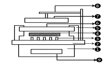
1) Equipment body
2) X-Y table
3) PCB Support
4) PCB
5) Stencil clamp
6) Stencil
7) Squeeze
8) Equipment robotic arm
9) Equipment control panel
1) Solder paste printing machine Equipment body: The body of the equipment primary houses three key parts, the power supply for the equipment, synchro motor and control circuitry. Power supply is for local power distribution to various parts of the equipment. Synchro-motor is used for movement of the robotic arm of the equipment. Control Circuitry is used for controlling speed, pressure in the z-direction, detection of presence of the PCB etc. Advanced and fully automatic equipment can self-adjust parameters including detection of adequate volume of solder paste available on the stencil. Fully automatic stencil printing machines have a safely cover and the equipment starts functioning only when the safety aver & closed.
• 1mil=(1/1000)1 inch
The equipment body also ensures stabilization of the equipment, and avoid unwanted movements during its operation.
2) X-Y table: Dimension of X-Y table determines the maximum size of PCB which can be printed using the solder paste printing machine. In X-Y table there are holes which are used to fix PCB support pins based on the dimension and any components already present on the PB. When solder paste is being printed on the PCB the squeezes puts pressure downwards in the Z-direction, the support pins ensure that the PCB does not bend due to this pressure. At any given point of time during its operation the stencil, PCB and the X-Y table are expected to be parallel to each other.
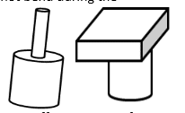
3) PCB support: As mentioned PCB support ensures PCB does not bend during the operation. There are different types of PCB support available. Some of the PCB are getting printed for second time i.e., bottom side of the PCB is already assembled with components and then the top-side of the PCB is being assembled. In such case the right type PCB support is selected to ensure existing components does not come Fig 12: Different types of PCB under stress during the solder paste printing process. Peg type, square type or serrated PCB support pins are available, however depending on type of components mounted a dimension of PCB customized PCB support can be fabricated.
In manual and semi-automatic solder paste printing equipment the PCB support pins needs to be manually fixed. In automatic solder paste printing equipment the equipment can be programmed to select and place the right PCB support required from a tray which holds all types of support.
4) PCB: It is important to note that the PCB Part number and revision are correct, the PCB is already baked. PCB is such ready state is Stacked and placed in the solder paste printing machine in the correct orientation. Alternatively, on automatic PCB stacker is used and it used to dispense PCB one-by-one into the automatic painting Machine. At this stage in some factories a bar-code label is placed for PCB and scanned for traceability purposes.
5) Stencil clamp: This is used for clamping the PCB in the right position so that during operation the stencil does not move. In automated equipment the machine adjusts the stencil automatically and clamping PCB’s have 3 fiducials in 3 corners of the PCB, stencil has opening at the fiducials locations which are matched with the PCB fiducial to ensure alignment.
6) Stencil: At this stage it is necessary to identify the right part number and revision is used.
7) Squeeze: The dimension of squeeze is verified whether it is “sufficient to cover the dimension of the PCB. Over a period of time due to repeated usage the squeeze tends to wear out leading to aberrations on the “printing blade” of the squeeze. If such aberrations noted than new squeeze should replace the defective one. It must also be verified that the squeeze being used is for the right process i.e., leaded squeeze for leaded process and lead-free squeeze for lead-free process. In several electronic manufacturing companies multiple types of leaded or lead-free solder paste is used in that case the squeeze is dedicated for each type of solder paste used in the process.
8) Equipment robotic arm: The robotic arm has clamping mechanism for holding the squeeze. In manual solder paste printing machines the robotic arm needs to be adjusted in Z-direction to provide adequate pressure on the stencil. In automatic solder paste printing machines z-direction is automatically set based on the pressure chosen for the printing operation.
9) Equipment control panel: The control panel is used to select the speed of operation, pressure to be deployed on the stencil etc. In automatic machines which has cleaning options, the control panel is also used to select the frequency of such cleaning operation.
With all the verification completed as mentioned above, the production supervisor authorizes first PCB printing. First PCB is printed and thoroughly inspected for orientation, misprint etc. In addition, a solder paste measuring equipment is used to measure the total volume of bolder deposited on CTQ (Critical To Quality) component lands. It defects are identified then necessary changes are made in the process then a new PCB is printed for first printing inspection. Subsequent to successful first printing go ahead is given for production.
Any misprinted PCB a thoroughly cleaned and dried either using manual methods or using stencil cleaning machine. Such cleaned PCB are thoroughly inspected before returning to the manufacturing process.
Typically, a fixed PCB is used repeatedly at the beginning of the solder printing process to avoid using and cleaning production PCB’s, Newer techniques like special films are available which are placed on top of the PCB’s and printed for first PCB verification.
All parameters for the solder paste printing operation are recorded and maintained as part of the enterprise resource planning system. Solder paste printing is also one of the key stages verified as part of In-process Quality Audit which is typically performed by the Process Engineering or the Quality department in the company.
Post successful solder paste printing the PCB moves to the next stage of component placement. The PCB’s printed with solder past within a few minutes completes the component placement and subsequent reflow stages to avoid “drying” of the paste


