

At the start of SMT Process there are key preparatory stages which contribute significantly to the manufacturing yield as well as the long term reliability of the electronics being manufactured. Ensuring right kitting and availability of the complete kit results in significant reduction of the DPMO (Defects Per Million Opportunities) achieved in process. Printed Circuit Boards are hygroscopic in nature and baking as per the design of the PCB or as per internationally accepted best practice is a recommended process to ensure several assembly defects during assembly are mitigated. Further, proper thawing of solder paste is a crucial step to ensure reliable solder paste printing and subsequent component placement and reflow.
PCB and Component kit preparation
As per production order the specific quantity of component as required in the Bill of Material (BOM) are retrieved from the warehouse. While such component retrieved is in progress the enterprise resource planning system also identifies whether there are already such component present in the manufacturing shop-floor which can be diverted for this kit request.
In preparation of a kit the component part number mentioned in the bill of material are strictly followed. An electronic component has a part number provided by the component manufacturer which is referred to as MPN: Manufacturer’s Part Number. Such MNP is mapped in the customer’s enterprise resource planning system to a CNP: Customer Part Number. Both the MNP and CNP is mapped to an EMPN: Electronic manufacturer’s Part Number. Such mapping brings in significant supply chain flexibility and visibility to the inventory available.
PCB on the other hand are custom designed and fabricated for a specific customer hence PCB’s typically have CPN and an EMPN only. Typically, the warehouse and shop-floor are seamlessly connected with necessary access control door in place. Since these two infrastructures are connected together, they form part of single Electrostatic Discharge Control grounding system. In such case additional protection for ESD may not be required for movement from warehouse to shop-floor.
In some cases, warehouse is port of a different building than the actual manufacturing shop-floor. In such cases guidelines laid out in ANSI ESD S20.20 for movement of Electrostatic sensitive Devices from an EPA (Electrostatic Discharge Protected Area) to a non-EPA and back inside an EPA needs to be followed.
If the component kit consists of Moisture Sensitive Components then the kit needs to be prepared with additional monitoring for exposure time. Component Moisture Sensitivity is pre-defined to various Moisture Sensitivity Levels (MSL’s).Industry guidelines classifies multi-layer PCB’s as MSL-3 hence necessary guidelines for such class needs to be followed.
Fully automated kitting mechanisms are available which are complemented with AGV’s (Automatic Guided Vehicles) for physical transport. Post such kits are complete the production team takes over responsibility of kit to verify a complete kit is available to start manufacturing. In some cases, due to procurement challenges a complete kit may not be available, in such cases cross-functional term takes disposition whether to proceed with manufacturing for a partially complete kit. Based on such disposition the kit is moved for production.
ML-PCB:-Multi layer Printed Circuit Board has more than 2 layers due to the complexity of the design. Some of the circuitry is spread across in the internal layers of the PCB
PCB Baking
Printed Circuit Board (PCB) is an interconnect structure supporting the traces which carry signal and power between the various components PCB also forms the support structure for the components which are moisture on either side. As mentioned earlier generally there are three types of Printed Circuit Boards: Rigid, Flexible and Semi-Rigid PCB’s. Depending on the product design PCB can be for high speed application high power applications, for control circuits etc. Also, some PCB’s are expected to function in high ambient temperature, vibration or moisture control. Also as mentioned earlier layers of design can be stacked on each layer from a multi-layered PCB.
Each layer of a PCB is formed of glass epoxy material placed within a structural mesh. Copper is etched on one side or both side of such structure depending on whether it is a single sided or double-sided PCB. As per the design requirement using photolithography techniques components pads (which are solderable surfaces) are formed. In the rest of
the part green epoxy ink is applied. A protective layer is formed either through electrolysis process or by physical deposition.
Because of this porous structure of PCB’s typically PCBs are vacuum sealed with desiccants. Even then due to handling at various stages PCB’s become expose to environment and thereby absorbs moisture. If Multi-layered PCB’s are subjected to thermal cycling then the entrapped moisture will evaporate and crack open the PCB surface in order to escape thereby damaging the PCB. Damage during assembly stage is very costly since the components are also assembled and the total damage cost shall include, cost of the PCB, cost of the assembled components as well as cost of processing and material handling. In some cases the moisture does not evaporate but causes internal cracks in the structure of the PCB. This is even more detrimental since this can possibly result in field failure.
Hence, both bare PCB’s as well as partially assembled PCB’s in WIP (Work in Progress) are baked before subjecting to thermal cycles. Depending on the size of the PCB and the number of layers following guiding table provides the temperature at which the PCB needs to be baked and duration of such baking.
Table:-1
| Dimension of PCB | Number of Layers | Temperature | Duration |
Solder Paste thawing
As mentioned earlier some PCB’s which are WIP are also needs to be baked since the PCB’s are already populated with component, the baking equipment needs to have necessary grounding to ensure that there are no chances for Electrostatic Discharge.
Post baking the PCB’s goes through a cooling cycle and immediately taken up for the next stage of production which is solder paste printing.
Solder Paste is a mixture of solder balls of a specific size mixed in a flux medium to form a homogeneous paste. To ensure homogeneity of solder paste it needs to be stored at temperature of <5°C. In additional to that solder paste in inventory needs to follow FIFO: First In First Out cycle.
Solder paste needs to be brought to room temperature before being be used in the solder paste printing machine. In order to do same first the solder paste is taken out from its colder storage and allowed to be kept in a cool place to ensure it starts attaining the shop-floor ambient temperature.
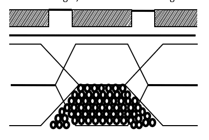
To ensure thawing of the solder paste a thawing equipment is used. Two containers of solder paste which are allowed in shop-floor ambient for a specific duration based on the temperature of the cold storage is placed in the thawing equipment. As shown in the Fig-9 the equipment is switched on after placing Fig-9: Typical thawing the two containers and closing the transparent lid. The spindle goes in a high speed rotation, the RPM and duration of spin & determined by the solder ball size in the paste and on the temperature at which the solder paste was being stored in the cold storage.

Once the rotation of the thawing equipment is completed the solder paste containers are taken out and carefully checked if there are 1) Any solid lumps 2) any bubbles present 3) any separation still found between the solder ball and flux. Based on the defect found disposition is taken to re-thaw the solder paste container or to reject the container.
There are different types of thawing equipment available based on: 1) The number of containers that can be placed in the equipment at a given time 2) single speed vs variable speed option. 3) Low maintenance option equipment (since solder paste may come outside the container and get deposited on parts of the equipment)
Once it is noted that solder paste of adequate quantity has been thawed the containers are taken to the next stage of solder paste printing.
 By: Ankan Mitra
The author is the Ex-president, SMTA INDIA CHAPTER

 Goes LIVE On Google Cloud Marketplace")


